| Creep
and Constitutive Models for Near-Eutectic SnPb
Overview
One lesson learned from SnPb studies is that here is no unique
constitutive model for SMT solder joints, thus the variety
of models available throughout the literature. In the end,
the applicability of a given model to real life assemblies
and a reasonable agreement between the ensuing life predictions
and test results determine whether a constitutive model will
be of use to design engineers and reliability analysts.
The mechanical behavior of solder depends on the joint microstructure
and is affected by many parameters such as intermetallics,
joint or specimen size, cooling rate of the assembly after
soldering, aging in service etc. Test factors such as specimen
or load eccentricity, temperature variations and measurement
errors also contribute to the scatter in the mechanical properties
of solder as is well known, for example, for steady state
creep. Nevertheless, simplified constitutive models have been
developed to help characterize the mechanical behavior of
SnPb solder and enable first-order stress/strain analysis
of solder joints using methods of classical mechanics or numerical
techniques such as the Finite Element Method (FEM).
What is Creep? |
| |
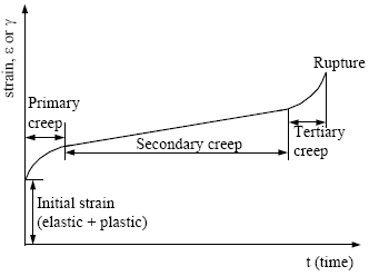
| Figure
1: Creep curve: strain versus time under constant
stress (or load) and temperature.
Under constant load or stress, solder undergoes progressive
inelastic deformations over time. This timedependent deformation
is called creep and the associated strains that develop over
time are creep strains. When the test specimen is subjected
to a constant load, the initial, instantaneous response includes
elastic and time-independent plastic flow. Creep then proceeds
in three stages of primary, secondary and tertiary creep (see
Figure 1). During primary creep, metals strain-harden. The
strain rate decreases over time, as hardening of the metal
becomes more difficult. Specimen deformations keep increasing
with secondary creep proceeding at a steady strain rate. Note
also that the initial deformation that occurs upon loading
of the test specimen includes both elastic and plastic strains.
Often, these initial deformations are not reported on in the
context of creep studies. However, they cannot be neglected,
a priori, because of the inelastic nature of the initial plastic
flow. Moreover, these initial deformations, which depend on
the loading rate, may become important under service conditions
with intermediate to rapid temperature ramps.
For most metals, secondary creep is the dominant deformation
mode at temperatures above half the melting point, TM , in
degree Kelvin. For eutectic SnPb, TM is 183°C =
456°K and 1/2 TM = 228°K = - 45°C.
That is, standard SnPb solder readily creeps at, and well
below, room temperature. The last stage of deformation is
tertiary creep where strain rates increase rapidly until the
test specimen ruptures. In SnPb solder, tertiary creep proceeds
by void formation and growth along grain boundaries, micro-cracking
and necking of tensile specimens.
Numerous researchers have investigated the mechanical and
creep behavior of near-eutectic SnPb solder (e.g., Baker
et al., 1973, Chen et al., 1971, Darveaux
et al., 1995, Grivas et al., 1979, Hacke
et al., 1993, Kashyap, 1981, Knecht et al.,
1991, Pao et al., 1992, Shine et al.,
1988, Stone et al., 1985/94, Wong et al.,
1988/90). Most investigations have focused on steady-state
creep, with the secondary creep rate often given as a function
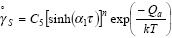
of stress and the absolute temperature, T: |
| |
(1) |
| special definitions: |
| |
 |
secondary creep rate |
|
| |
A |
a material constant |
|
| |
b |
dislocation characteristic length or magnitude of Burgers
vector |
|
| |
g |
the material's grain size |
|
| |
T |
temperature |
|
| |
E(T) |
the temperature dependent Young’s modulus |
|
| |
k |
is Boltzman’s constant |
|
| |
 |
stress |
|
| |
p and n |
constant exponents |
|
| |
Q |
the activation energy of the rate controlling diffusion mechanism |
|
|
Equation (1) is known as Dorn’s equation (Bird et al.,
1969) and is often simplified as: |
 |
(2) |
| special definitions: |
| |
A1 |
another material constant |
|
| |
Qa |
an apparent activation energy |
|
|
Equation (2) shows the strong dependence of creep rates on
stress and temperature as well as grain size (in the case
of SnPb solder).
Since creep properties, as well as strength and other mechanical
properties, vary with specimen size, the mechanical response
of tiny solder joints differs from that of bulk solder test
specimens. For engineering applications dealing with surface-mount
(SM) assemblies, constitutive models developed from measurements
on solder joint specimens have proven to be very useful. Solder
deformations, including creep, have been measured on solder
joints of actual electronic assemblies (e.g., Shine and Fox,
1988, Knecht and Fox, 1991) and for several solder alloys:
60Sn-40Pb, 62Sn-36Pb-2Ag, 96.5Sn-3.5Ag,
97.5Pb-2.5Sn, 100In and 50In-50Pb
(Darveaux et al., 1995). These models are presented, briefly,
hereafter because they have been found to be of use to practicing
engineers. The reader is referred to the original publications
for additional details as well as for relevant information
on the experimental techniques that were used and that could
be applied to the study of lead-free solders.
Motorola / Darveaux's Constitutive
Model
Darveaux and his co-workers at Motorola (Darveaux et al.,
1995) conducted extensive mechanical testing of flip-chip
and Ball Grid Array (BGA) solder joints and characterized
the time-independent plastic flow and creep deformations of
several solder alloys. Their constitutive model is described
below for several alloys of electronic solder. Robert Darveaux
implemented this model into two commercial finite element
codes, ANSYSTM and ABAQUSTM. His original
publication (Darveaux et al., 1995, Chapter 13 in Ball Grid
Array Technology) includes detailed recommendations on how
to input material constants in the preprocessor of those two
programs. One important feature of Darveaux’s creep
model is that it was found to apply consistently to several
solder alloys: 60Sn-40Pb, 62Sn-36Pb-2Ag,
96.5Sn-3.5Ag, 97.5Pb-2.5Sn, 100In
and 50In-50Pb, and over a wide range of temperatures
and several orders of magnitude in strain rates.
The initial, instantaneous strain that develops at the start
of a creep test includes an elastic strain and an inelastic
strain that represents time-independent plastic flow. The
plastic strain is described by a plastic flow or strain hardening
law of the form: |
 |
(3) |
| special definitions: |
| |
 |
plastic strain |
|
| |
C6 and m |
material constants |
|
| |
 |
applied stress |
|
| |
G=G(T) |
temperature-dependent shear modulus
given as: |
|
 |
(4) |
| |
G0 |
shear modulus at 0°C |
|
| |
G1 |
shear modulus temperature coefficient |
|
| |
|
G0 = 1.9 Mpsi and G1
= 8.1 kpsi/°K for both alloys of 60Sn-40Pb
and 62Sn-36Pb-2Ag |
|
|
The elastic constants and the plastic flow parameters for
several solder alloys, including SnAg eutectic, are given
in Table 1 below. Note that the elastic constants and the
power-law exponent m are about the same for 60Sn-40Pb
and 62Sn-36Pb-2Ag. However, the constant C6
is about twice as low for 62Sn-36Pb-2Ag. Under
equal loads, tin-lead with 2% silver will see half as much
initial plastic strain than 60Sn-40Pb.
|
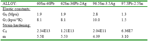 |
| Table 1:
Solder material constants for shear modulus and plastic flow
rule (after Darveaux et al., 1995).
During primary or transient creep, the creep strain is given
by the equation: |
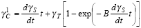 |
(5) |
| special definitions: |
| |
 |
primary creep strain |
|
| |
 |
transient creep strain |
|
| |
B |
transient creep coefficient |
|
| |
 |
steady state creep
rate |
|
The primary creep constants for several alloys are given
in Table 2.
|
 |
Table 2:
Primary creep constants for common solder alloys (after Darveaux
et al., 1995).
The primary creep rate is: |
| |
(6) |
Initially, at time t = 0, the primary creep rate is a factor
 times greater than the steady state creep rate. For 60Sn-40Pb,
this factor is:
= 1 + 0.026 x 403 = 11.48, i.e., the initial transient creep
rate is over an order of magnitude higher than the steady
creep rate. For Sn-3.5Ag, the rate factor is even larger:
= 1 + 0.167 x 131 = 21.88. Thus, primary creep may not
be negligible in applications with high temperature ramp rate
or under thermal cycling conditions with short dwell times.
times greater than the steady state creep rate. For 60Sn-40Pb,
this factor is:
= 1 + 0.026 x 403 = 11.48, i.e., the initial transient creep
rate is over an order of magnitude higher than the steady
creep rate. For Sn-3.5Ag, the rate factor is even larger:
= 1 + 0.167 x 131 = 21.88. Thus, primary creep may not
be negligible in applications with high temperature ramp rate
or under thermal cycling conditions with short dwell times.
More general relationships were found to apply to steady
state creep of solder in shear: |
 |
(7) |
| or in a simplified form: |
 |
(8) |
| special definitions: |
| |
 |
steady state strain rate |
|
| |
G(T) |
temperature-dependent shear modulus |
|
| |
T |
absolute temperature (in degree Kelvin) |
|
| |
|
applied stress |
|
| |
n |
constant exponent that depends on
the controlling creep mechanism |
|
| |
k |
Boltzmann’s constant (k = 8.620
x 10-5 eV/°K) |
|
| |
Q |
creep activation energy |
|
| |
Qa |
apparent activation energy |
|
| |
 ,
C4, C5 ,
C4, C5 |
constants |
|
The above constants and activation energies are given for
several solder alloys in Table 3.
|
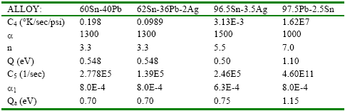 |
Table 3: Steady state creep parameters
for common solders (after Darveaux et al., 1995).
DEC's Model
Knecht, Fox and Shine of the Digital Equipment
Corporation (DEC) conducted isothermal mechanical and fatigue
testing of 63Sn-37Pb solder joints on a 7.6 m x 7.6 mm,16
I/O Leadless Ceramic Chip Carrier (LCCC) test vehicle (Shine
et al., 1988, Knecht et al., 1991). The LCCCs were mounted
on stainless steel or G-10 organic substrates with copper
pads matching the component terminations (0.64 x 1.0 mm
pads). Solder joint thickness varied from 4 to 12 mil. Testing
was conducted at temperatures of 25°C, 60°C and
100°C. The solder joints were subjected to shear in
a torsion apparatus powered by an electric motor. Shear
deformations were determined from the reflection of a laser
beam on the mirrored edges of LCCC components. Creep data
was obtained from curves of isothermal creep strain versus
time under constant applied torques. Stable stress/strain
hysteresis loops were obtained from the first cycles of
fatigue tests conducted under constant plastic strain range.
From these experiments, and associated data reduction, failure
mode analysis and modeling, Shine and Fox (Shine et al.,
1988) concluded the following:
|
| |
- Grain boundary creep at low stresses and creep rates.
- Matrix creep at high stresses and creep rates.
|
- Solder joints undergo creep-fatigue failures associated
with steady-state creep. Creep damage occurs by a combination
of grain-boundary and matrix creep, with Scanning Electron
Microscope (SEM) photos of fatigued solder joints showing
intercrystalline voids and cracks. Isothermal fatigue life
cycles have an inverse relationship to integrated matrix
creep.
- The grain size of thick joints is larger than that of
thin joints and solder grain size increases during fatigue
testing. Under identical loads, thin joints with initially
smaller grain sizes are expected to have a longer fatigue
life than thick joints with larger grains.
Using the hysteresis loops and creep data from the above
experiments, Knecht and Fox (Knecht et al., 1991) developed
a simple constitutive model for eutectic (63Sn-37Pb)
solder in shear. The constitutive equations from that study
are summarized hereafter with some minor modifications. Knecht
and Fox used their model to conduct finite element analysis
of solder joints in SMT assemblies and to correlate fatigue
life data to integrated matrix creep strains.
The average shear strain is given as the sum of an elastic
strain, a time-independent plastic strain, and
a secondary creep strain, that is: |
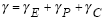 |
(9) |
| special definitions: |
| |
 |
shear strain |
|
| |
 |
elastic strain |
|
| |
|
time-independent plastic strain |
|
| |
 |
secondary creep strain |
|
The elastic strain component is: |
 |
(10) |
where the temperature dependent shear modulus is: |
 |
(11) |
Poisson's ratio for near-eutectic solder is  =
0.4 and the temperature-dependent Young's modulus is: =
0.4 and the temperature-dependent Young's modulus is: |
 |
(12a) |
| or: |
 |
(12b) |
The time-independent plastic strain is given by the following
plastic flow rule: |
 |
(13) |
| special definitions: |
| |
 |
temperature-dependent plasticity
parameter |
|
where the temperature-dependent plasticity parameter is obtained
by curve-fitting the plasticity parameter versus temperature
data in the original publication by Knecht and Fox (1991),
i.e.: |
 |
(14) |
Finally, creep strains are obtained by integration of the
steady state creep rate equations: |
 |
(15) |
| or |
 |
(16) |
The first term on the right-hand-side of equations (15) and
(16) is for grain boundary creep with a stress exponent: nGB
= 2 and an activation energy:  HGB
= 0.5eV. The second term on the right-hand-side of
(15) and (16) is for matrix creep with a stress exponent:
nMC = 7.1 and an activation energy:
HGB
= 0.84eV. As shown by Knecht and Fox, these values
of stress exponents and activation energies are consistent
with steady state creep parameters reported in the literature
(see Table 4 below). HGB
= 0.5eV. The second term on the right-hand-side of
(15) and (16) is for matrix creep with a stress exponent:
nMC = 7.1 and an activation energy:
HGB
= 0.84eV. As shown by Knecht and Fox, these values
of stress exponents and activation energies are consistent
with steady state creep parameters reported in the literature
(see Table 4 below).
|
| |
Table 4: Comparison of near-eutectic SnPb
creep parameters (after Knecht et al., 1988).
Last, note that, even though the experimental
results of Shine and Fox (Shine et al., 1988) suggest a
grain size effect, the constitutive model developed by Knecht
and Fox does not include any grain size parameter. The most
likely reason for this is that those effects are difficult
to quantify when the grain size is not a control parameter
of an experiment. However, Knecht and Fox stated that "using
"real" joints will generate practical results"
(Knecht et al., 1991) and their constitutive model is thought
to be useful for the engineering analysis of solder joints.
|
| Hughes' Creep
Model |
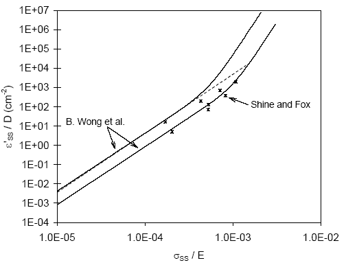 |
Figure 2: Creep rate plot for Pb/Sn eutectic
solder.
Boon Wong and his colleagues at Hughes Aircraft
Company (B. Wong et al., 1988) compiled Sn-Pb eutectic steady
state creep data from seven sources. The data, which covered
several orders of magnitude in stress and creep rates, was
found to fit in a correlation band as shown in Figure 2.
The raw data fell within a band of height about one order
of magnitude in the vertical direction. The width and height
of the band are typical of the scatter usually associated
with creep data. Available data points from Shine and Fox
(Shine et al., 1987) are found to fit within or close to
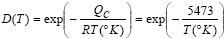
Wong's correlation band. In Figure 2, the normal stress,
sSS, is scaled with a temperature-dependent Young's modulus,
E = E(T), on the horizontal axis. Young's modulus is given
as in equation (12a). The steady state creep rate on the
vertical axis is normalized with a Arrhenius-type, temperature-dependent
diffusion parameter, D = D(T):
|
 |
(17) |
| special definitions: |
| |
QC |
average activation energy for
creep of eutectic SnPb solder: QC = 45 kJ/mole
= 0.47eV |
| |
R |
universal gas constant: R
= 8.314 J/°K.mole. |
|
The correlation band in Figure 2 has two distinct slopes
that reflect different creep mechanisms:
- A dislocation glide regime with a stress exponent of 3
in the low stress region.
- A dislocation climb regime with a stress exponent of 7
in the higher stress region.
Based on the above correlation of creep data, Wong gave the
following expression for average creep rates: |
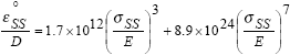 |
(18) |
The equations of the lower and upper bounds of the correlation
band are (Clech et al., 1988): |
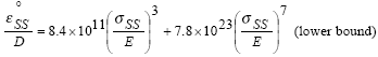 |
(19) |
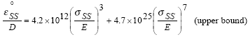 |
(20) |
The above stress exponents are consistent with the steady
state creep equation in DEC's steady state creep model. Note
also that Wong's creep rate equations do not include grain
size dependence either. Wong argued that the experimental
data was inconclusive at the time (Wong et al., 1988) and
this did not warrant any attempt at including grain size effects.
Wong also stated that grain size dependence is not expected
in either the climb or glide-controlled creep regimes. One
last important aspect of Wong's steady state creep model is
that it was derived based on the correlation of creep data
from several independent sources, with the correlation holding
over a wide range of temperatures (-60°C to 150°C),
stresses and creep rates.
The above compilation of creep data has been used successfully
in a solder joint life prediction model developed by Wong
et al., 1988. The upper bound of the correlation band was
also used as the creep rate equation in the Solder Reliability
Solutions (SRS) life prediction model (Clech, 1996). The upper
bound was selected in order to maximize strain rates, thus
building in some conservatism in the model. The SRS model
has since been validated by over sixty experiments (Clech,
2000).
Based on Sn-Pb experience, we can expect creep rates from
compiled test results for lead-free solders to spread over
one order of magnitude. Such spread in the data did not impede
the development of useful, first-order solder joint life prediction
models for Sn-Pb assemblies.
Hall's Stress / Strain Hysteresis
Loop
One of the most significant contributions to the field of
solder joint mechanics, and also most enjoyable reading (in
this author’s opinion), is the shear strain and hysteresis
loop measurements and theory developed by Peter Hall at AT&T
Bell Laboratories (Hall, 1984 and 1991). Using strain gauge
measurements and a simplified analysis of shear forces exerted
on the solder joints of LCCC assemblies, Hall showed that
the stress/strain response of solder joints during temperature
cycling is a hysteresis loop (see Figure 2). The shape of
the loop reflects the temperature-dependent inelastic deformations
of solder and elastic deformations of the entire assembly.
The thermal expansion mismatch between board and component
is accommodated by shear of the solder joints and simultaneous
stretching and bending of the board and component. These elastic
deformations of the interconnected parts provide compliance
to the assembly, suggesting practical ways to reduce solder
joint stresses by designing boards and components that are
more compliant.
|
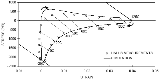 |
Figure 3: Solder joint hysteresis loop
during thermal cycling between -25°C and 125°C.
The hysteresis loop in Figure 3 illustrates
the complexity of the solder joint stress/strain response
during a large temperature cycle between -25°C and 125°C.
The dwell times at the temperature extremes were two hours.
The ramp times were five hours with a rather slow ramp rate
of 0.5°C/minute. The data points, shown as circles,
are derived from Hall's strain measurements on non-castellated,
25-mil pitch, 84 I/O LCCCs mounted on FR-4. The solder joints
were 11 mil high. A complete description of test vehicles
and details of the experimental set-up, measurement techniques
and data reduction procedures are given in Hall's publications
(Hall, 1984, 1987, 1991). Pao conducted similar measurements
on a double-beam, alumina on aluminum test vehicle (Pao
et al., 1987).
The shape of the hysteresis loop in Figure
3 reflects the non-linear, temperature-dependent constitutive
behavior of solder. Important features of the loop are described
hereafter:
-
The loop is described clock-wise. Isothermal
stress reduction lines are drawn as dashed lines between
the data points corresponding to equal temperatures during
the ramp-up and ramp-down phases of the thermal cycle.
The stress reduction lines are shown for every 10 or 20°C
temperature increment. The stress reduction lines are
almost parallel to each other, with an average slope in
very good agreement with the slope predicted by Hall’s
assembly stiffness model.
- During the dwell periods at the temperature extremes,
stresses are reduced along the stress-reduction lines (shown
as solid lines) for those temperatures:
|
| |
- At 125°C, where solder is very soft, shear strains
are large and initial stresses are relatively low, less
than 200 psi. Creep rates are very high and stress reduction
is rapid. The intersect of the stress reduction line with
the strain axis is the maximum available strain due the
thermal expansion mismatch between the board and the LCCC
component.
- At -25°C, initial stresses are much higher, of the
order of -2300 psi. In spite of high stresses, there is
not much stress reduction during the two-hour dwell because
creep rates are rather small at cold temperatures.
|
- During the ramp-up phase of the thermal cycle:
|
| |
- As temperature goes up, starting at -25°C, solder
is relatively strong and the shear strain remains about
constant. Actually, shear forces are unloaded almost elastically.
- Past about 35°C, where the shear force is zero, stresses
build up due to plastic flow of solder in the opposite direction
and strains start increasing with the added thermal expansion
mismatch between board and component.
- Creep accelerates as temperature keeps going up. Slightly
past 50°C, the creep rates are so high that stress reduction
prevents any further build-up of stress. Creep strains develop
at a faster rate, contributing to rapid increments in the
total shear strain.
- When temperature approaches 125°C, strains keep increasing
with the thermal expansion mismatch between board and component
and stresses relax at a rather fast rate.
|
- During the ramp-down phase of the thermal cycle:
|
| |
- As temperature goes down, starting at 125°C, the
cycle is reversed and shear strains decrease.
- Initially, and down to about 50-60°C, shear strains
decrease at a high rate. Stresses start building up in the
opposite direction.
- From 50-60°C to -25°C, stresses become larger
and built up at faster rate since solder becomes stronger
at lower temperatures.
|
| The simulated loop shown in Figure
3 was generated using the plastic flow rule and creep constitutive
model from DEC. Loop simulations have been conducted by several
investigators using slightly different approaches and constitutive
models (e.g., Sherry and Hall, 1986, Clech et al., 1987, Lovasco,
1988, Subrahmanyan et al., 1989, Wilcox et al., 1989, Li et
al., 1991, Whalley et al., 1989/91, Lau and Pao, 1997). |
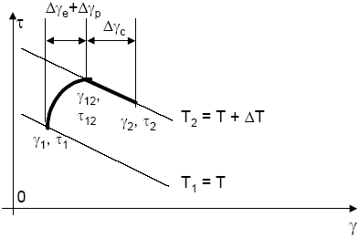 |
Figure 4:
Solder joint stress/strain simulation when temperature increases
from T to (T + T).
The basic algorithm that is used to generate stress/strain
hysteresis loops during thermal cycling follows the stress/strain
curves shown in Figure 4. During a small time-step from time
t to (t +  t),
temperature increases from T to (T + T).
At time t, the stress/strain curve intersects the stress reduction
line for temperature T1 = T. Due to the increase
in temperature, stresses build-up instantaneously from 1
to 12
with a change in strain from 1
to 12
that includes an elastic strain increment e
and plastic flow with a strain increment p.
Stresses then relax from 12
to 2,
and the shear strain increases by creep (increment c)
along the stress reduction line at temperature T2
= (T + T).
Knowing the stress / strain state (1,
1)
at time t, the stress / strain state (2,
2)
at time (t + t)
is obtained by solving the following system of four equations
with four unknowns 12,
12,
2,
and 2: t),
temperature increases from T to (T + T).
At time t, the stress/strain curve intersects the stress reduction
line for temperature T1 = T. Due to the increase
in temperature, stresses build-up instantaneously from 1
to 12
with a change in strain from 1
to 12
that includes an elastic strain increment e
and plastic flow with a strain increment p.
Stresses then relax from 12
to 2,
and the shear strain increases by creep (increment c)
along the stress reduction line at temperature T2
= (T + T).
Knowing the stress / strain state (1,
1)
at time t, the stress / strain state (2,
2)
at time (t + t)
is obtained by solving the following system of four equations
with four unknowns 12,
12,
2,
and 2:
- From the stress reduction line at T2 = (T + T):
|
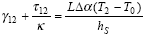 |
(21) |
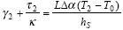 |
(22) |
|
- For the strain increment due to elastic deformation and
plastic flow as per, for example, DEC's plastic flow rule:
|
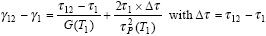 |
(23) |
|
- For the creep strain developing during the short dwell
of duration t
at T2:
|
 |
(24) |
| special definition: |
| |
 |
steady state creep
rate under an applied stress 12
at temperature T2 |
The above algorithm can be implemented in a computer program
or even in a spreadsheet. Usually, a zero stress / strain
state is used, somewhat arbitrarily, to initialize the algorithm.
Small enough time steps are required to follow the prescribed
temperature profile closely and to generate the stress / strain
response with the desired accuracy. A few cycle iterations
are typically required to obtain a closed and stable hysteresis
loops for stiff systems like leadless assemblies. Many more
iterations are needed for compliant systems like leaded assemblies
with very compliant leads. Hysteresis loops can also be obtained
using finite element models that include material options
for a constitutive model with elastic, plastic flow and creep
(see, for example, Darveaux et al., 1995/97, Lau and Pao,
1997). |
|